Digital image processing technology has been widely used in the field of electronic communication and information processing. It is of great practical significance to design a video signal acquisition circuit that is flexible, easy to use and easy to embed into the system.
In the research of DSP-based video surveillance system, considering the specific requirements of high-speed real-time processing and practical application, it is necessary to develop a video image signal acquisition system with high speed and high integration. The decoder chip and the complex programmable logic device (CPLD) form the front-end image acquisition part. The design uses a dedicated video decoding chip, with CPLD device as the control unit and peripheral interface, with FIFO as the cache structure, which can effectively realize the high-speed parallel of video signal acquisition and reading, with simple overall circuit, high reliability and integration. The advantages of high interface and convenient interface can be applied to various video signal processing systems without changing the hardware circuit. The original very complex circuit design has been greatly simplified, and the original pure hardware design has become a hybrid design of software and hardware, which makes the design of the whole system more flexible.
1 system hardware platform structure
The hardware structure of the system platform is shown in Figure 1. The whole system is divided into two parts, namely the image acquisition system and the DSP-based main system. The former is a high-speed video acquisition system based on SAA7110A/SAA7110 video decoding chip, which is accurately sampled by complex programmable logic chip CPLD; the latter is a general-purpose digital signal processing system, which mainly includes: 64K WORD program memory, 64K WORD data memory, DSP, clock generation circuit, serial interface and corresponding level conversion circuit.
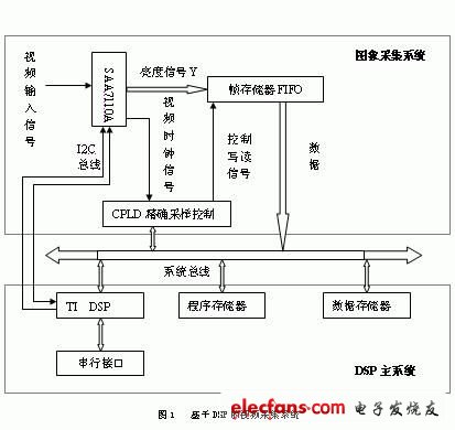
The workflow of the system is that the video image data of the specified area is accurately captured by the image acquisition system in the QCIF format, and temporarily stored in the frame memory FIFO; the data temporarily stored in the FIFO is read into the data memory of the DSP by the DSP. The H.263-based video data compression is performed together with the original several frames of image data; then the compressed video data is smoothly output from the serial interface by the DSP, and transmitted to the remote monitoring center by the ordinary MODEM or ADSL MODEM. After receiving the data, the PC of the monitoring center performs corresponding decoding, and displays the restored video image or performs WEB-based broadcasting.
2 video signal acquisition system
2.1 Basic characteristics of video signal acquisition system
The general video signal acquisition system generally consists of a video signal through clamp amplification, synchronization signal separation, luminance/chrominance signal separation and A/D conversion, etc. The sampled data is output to the data bus according to a certain timing and bus requirements. Thereby, the decoding of the video signal is completed, and the memory in the figure is used as a frame sampling buffer memory, and can adapt to the bus interface of different bus, output format and timing requirements.
The video signal acquisition system is a special case of a high speed data acquisition system. In the past, video signal acquisition systems used small-scale digital and analog devices to achieve high-speed operational amplification, synchronization signal separation, luminance / chrominance signal separation, high-speed A / D conversion, phase-locked loop, sequential logic control and other circuits. However, since the sampling frequency and operating clock of the system are as high as tens of megahertz, and the device integration is low, the wiring is complicated, and the coupling interference between the stages and devices is large, development and debugging are very difficult; on the other hand, in order to achieve accurate sampling. Therefore, the sampling clock needs to be in a synchronous relationship with the input video signal. Therefore, using the separated synchronization signal and the system sampling clock for phase locking to generate a precisely synchronized sampling clock becomes another difficulty in the design and debugging process. At the same time, by implementing the programmable control of brightness, chromaticity, contrast, and video pre-amplification gain, the intelligence of video signal acquisition is achieved, which is difficult to accomplish in the past. In this regard, there has been a deep understanding of the initial development of the system [1].
Based on the above considerations, the system uses the SAA7110A as the input front-end video sampling processor of the video surveillance system.
2.2 Video image acquisition system design
The SAA7110/SAA7110A is a highly integrated, fully functional, large-scale video decoding integrated circuit [2]. It is packaged in PLCC68. It integrates two 8-bit A/D converters for video signal sampling, clock generation circuit and peripheral circuits such as brightness, contrast and saturation control. It replaces the original discrete circuit and greatly reduces it. Small system design workload, and flexible configuration of functions through a large number of built-in functional circuits and control registers. The SAA7110/SAA7110A can be applied in the fields of desktop video, multimedia, digital television, image processing, video telephony, video image acquisition systems, and the like.
The control bus interface of the SAA7110/SAA7110A is the I2C bus. As a slave device of the I2C bus, the SAA7110/SAA7110A can be set to 9CH/9DH (W/R, SA=0) or 9DH/9FH (W/R, SA= according to the level of the SA pin. 1). There are a total of 47 registers inside, which control the decoder (00H to 19H) and the video interface (20H to 34H). Input channel selection, level clamp and gain control, brightness, chrominance and saturation control can be performed by reading and writing the above registers in the chip through the I2C bus.
However, there is a problem that must be solved, that is, the DSP chip does not have a built-in I2C bus interface. To this end, the system proposes and adopts a software simulation of two programmable I/O pins of the DSP chip to implement the I2C bus control method. . Due to the limitation of the C2000 program storage space of only 64KB, in order to reduce the scale of the I2C bus control simulation software, the simulation software is all completed in assembly language, which brings considerable difficulty and workload to the design of the system.
Name:150/250V PVC insulated shipboard control cable
Model:DA/SA/NSA/NA type:CKVV, CKVV80, CKVV90, CKVV82, CKVV92
Name:150/250V XLPE insulated shipboard control cable
Model:DA/SA/NSA/NA type:CKJV, CKJV80, CKJV90, CKJV82, CKJV92, CKJ82, CKJ92
SC/NC/NSC type:CKJPF, CKJPF80, CKJPF90, CKJPF86, CKJPF96, CKJ86, CKJ96
CKJPFP, CKJPFP80, CKJPFP90, CKJPFP86, CKJPFP96, CKJP86, CKJP96
CKJPJ, CKJPJ80, CKJPJ90, CKJPJ85, CKJPJ95, CKJ85, CKJ95
CKJPJP, CKJPJP80, CKJPJP90, CKJPJP85, CKJPJP95, CKJP85, CKJP95
Specification:(2~37)×(0.5~2.5)mm2
Executive Standards:IEC60092-350, IEC60092-376
Application:The cable is intended for control system or shipboard and offshore building
Fire Resistant Marine Control Cable
Marine Cable,Fire Resistant Marine Control Cable,Ship Control Cable,Xlpe Control Cable
Jiangsu Jiangyang Special Cable Co,.Ltd. , https://www.jymarinecable.com