Although there are still many uncertainties in the design of radio frequency (RF) circuit boards in theory, there are still many rules that can be followed in the design of RF circuit boards. However, in the actual design, the really practical skill is how to trade off these rules when they cannot be implemented due to various restrictions. This article will focus on various issues related to the design of the RF circuit board partition.
01
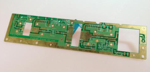
Types of micro vias
Circuits of different nature on the circuit board must be separated, but they must be connected under the best circumstances without electromagnetic interference, which requires the use of microvias. Usually the diameter of micro vias is 0.05mm~0.20mm. These vias are generally divided into three categories, namely blind vias, bury vias and through vias. Blind holes are located on the top and bottom surfaces of the printed circuit board and have a certain depth. They are used to connect the surface line and the underlying inner line. The depth of the hole usually does not exceed a certain ratio (aperture). Buried hole refers to the connection hole located in the inner layer of the printed circuit board, which does not extend to the surface of the circuit board. The above-mentioned two types of holes are located in the inner layer of the circuit board, and are completed by a through-hole forming process before lamination, and several inner layers may be overlapped during the formation of the via. The third type is called a through hole, which penetrates the entire circuit board and can be used for internal interconnection or as an adhesive positioning hole for components.
02
Use partitioning techniques
When designing the RF circuit board, the high-power RF amplifier (HPA) and the low-noise amplifier (LNA) should be separated as much as possible. Simply put, keep the high-power RF transmitter circuit away from the low-noise receiver circuit. If there is a lot of space on the PCB, this can be easily done. But usually when there are many components, the PCB manufacturing space becomes very small, so this is difficult to achieve. You can put them on both sides of the PCB board, or let them work alternately instead of working at the same time. High-power circuits sometimes include RF buffers and voltage-controlled oscillators (VCO).
Design partitions can be divided into physical partitioning and electrical partitioning. Physical partitioning mainly involves issues such as component layout, orientation, and shielding; electrical partitioning can continue to be divided into power distribution, RF wiring, sensitive circuits and signals, and grounding.
03
Physical partition
Component layout is the key to achieving an excellent RF design. The most effective technique is to first fix the components on the RF path and adjust their position to minimize the length of the RF path. And keep the RF input away from the RF output, and as far away as possible from high-power circuits and low-noise circuits.
The most effective circuit board stacking method is to arrange the main ground on the second layer below the surface, and route the RF lines on the surface as much as possible. Minimizing the size of the vias on the RF path can not only reduce the path inductance, but also reduce the virtual solder joints on the main ground and reduce the chance of RF energy leaking to other areas of the laminate.
In physical space, linear circuits like multi-stage amplifiers are usually sufficient to isolate multiple RF zones from each other, but duplexers, mixers, and intermediate frequency amplifiers always have multiple RF/IF signals that interfere with each other. Therefore, care must be taken to minimize this effect. RF and IF traces should be crossed as much as possible, and a grounding area should be placed between them as much as possible. The correct RF path is very important to the performance of the entire PCB board, which is why component layout usually takes up most of the time in the mobile phone PCB board design.
On the mobile phone PCB board, usually the low-noise amplifier circuit can be placed on one side of the PCB proofing board, and the high-power amplifier on the other side, and finally they are connected to the RF antenna on the same side by a duplexer. One end and the other end of the baseband processor. This requires some skill to ensure that RF energy does not pass through the vias from one side of the board to the other. A common technique is to use blind holes on both sides. The adverse effects of vias can be minimized by arranging blind vias in areas where both sides of the PCB are free from RF interference.
04
Metal shield
Sometimes, it is not possible to keep enough separation between multiple circuit blocks. In this case, it is necessary to consider using a metal shield to shield the RF energy in the RF area. However, metal shields also have side effects, such as manufacturing The cost and assembly cost are both high.
It is difficult to guarantee high precision for metal shielding covers with irregular shapes during manufacture. Rectangular or square metal shielding covers also restrict the layout of components; metal shielding covers are not conducive to component replacement and malfunction displacement; metal shielding covers must Solder on the ground plane, and must maintain a proper distance from the components, so it takes up valuable PCB board space.
It is very important to ensure the integrity of the metal shield as much as possible, so the digital signal lines entering the metal shield should go as far as possible to the inner layer, and it is best to set the next layer of the signal circuit layer as the ground layer. The RF signal line can be routed out from the small gap at the bottom of the metal shield and the wiring layer at the grounding gap, but the gap should be surrounded by a large grounding area as much as possible. The grounding on different signal layers can use multiple vias Linked up. Despite the above shortcomings, metal shields are still very effective and are often the only solution to isolate critical circuits.
05
Power decoupling circuit
Appropriate and effective chip power decoupling circuit is also very important. Many RF chips that integrate linear circuits are very sensitive to power noise. Usually, each chip needs to use up to four capacitors and an isolation inductor to filter out all power noise.
The minimum capacitance value usually depends on the resonant frequency of the capacitor itself and the pin inductance, and the value of C4 is selected accordingly. The values ​​of C3 and C2 are relatively large due to their own pin inductance, so the effect of RF decoupling is worse, but they are more suitable for filtering lower frequency noise signals. RF decoupling is done by the inductor L1, which prevents the RF signal from coupling to the chip from the power line. Because all traces are a potential antenna that can both receive and transmit RF signals, it is necessary to isolate RF signals from key circuits and components.
The physical location of these decoupled components is usually also critical. The layout principles of these important components are: C4 must be as close to the IC pin as possible and grounded, C3 must be the closest to C4, C2 must be the closest to C3, and the connection trace between the IC pin and C4 should be as short as possible. The ground terminal of each component (especially C4) should usually be connected to the ground pin of the chip through the first ground layer under the board. The via that connects the component to the ground plane should be as close as possible to the component pad on the PCB. It is best to use blind holes made on the pad to minimize the inductance of the connection line. The inductance L1 should be close to C1.
An integrated circuit or amplifier often has an open collector output (open collector), so a pullup inductor is needed to provide a high impedance RF load and a low impedance DC power supply. The same principle applies to this The power supply side of the inductor is decoupled. Some chips require multiple power supplies to work, so two or three sets of capacitors and inductors may be required to decouple them separately. If there is not enough space around the chip, the decoupling effect may be poor. Especially need to pay special attention to: the inductances are rarely close together in parallel, because this will form an air-core transformer and induce interference signals with each other, so the distance between them must be at least the height of one of them, or at a right angle Arrange to minimize mutual inductance.
Handheld Fan Mini Portable Fan Powerful Personal Fans Speed Adjustable Battery Operated Type-C Rechargeable Eyelash Fan for Kids Women Men Indoor Outdoor Travel Cooling.
Mini Type-C Rechargeable Fan] cooling desk fans are built with 1200mAh rechargeable lithium battery, 3 adjustable speeds, fully charges in 3 hours, wireless working time 3-10hours. The lanyard design frees your hands and perfect for traveling
[3 Adjustable Speed & Enjoy Cool Summer]3 Adjustable Speed Level -- natural wind/cool wind/strong wind, just adjust the appropriate fan speed by pressing the power button repeatedly. Equipped with 3pcs fan blades which are made of ABS material, strong and durable produces a strong and soft airflow. Never worry about the outdoors even the temperature is so high. Just enjoy your cooling summer with this must-have
[Convenient design of portable fan]The mini fan weighs only 90 grams, That you can hang it around your neck with a lanyard without any pressure. Even if your child uses it, it will not bear weight pressure. You can put it in a backpack or handbag or even in your pocket when traveling outdoors. This simple and compact design is particularly suitable for summer travel or outdoor sports.
[Rechargeable Battery & Energy Source]The Type-C electric fan can be recharged with Type-C charger, laptop, computer, power bank, car power ban and other Type-C enable devices. A happy and lasting family journey
[Perfect Gift & After-sales]You can get a portable rechargeable fan, a Type-C cable, a lanyard, a fan stand and a User guide in the package. It's definitely a perfect gift idea for your families, friends, or your loved ones.
Rechargeable Small Pocket Fan,Handheld Mini fan, 3 In 1 Portable Type-C Mini fan
Shenzhen Focras Technology Co.,Ltd , https://www.focrass.com