The control circuit of the full-bridge topology designed in this paper consists of several key components, including the controller, protection circuit, current feedback, voltage feedback, drive circuit, and auxiliary power supply. As the core of the switching power supply, the control circuit plays a vital role in determining the overall performance of the system. Various parameters such as constant voltage and constant current regulation, ripple size, and input/output characteristics are closely tied to the design of the control circuit. Additionally, since the main circuit uses a full-bridge topology, it is crucial to implement measures that prevent shoot-through phenomena during operation. The following sections provide a detailed description of each functional component within the control circuit.
Introduction to Current Control Chip
The UC3846 is selected as the primary control chip for this design. It features a high-current totem-pole output, capable of driving FETs directly with a peak output current of 500mA. The chip includes an internal precision bandgap reference, a high-frequency oscillator, an error amplifier, a differential current-sense amplifier, a voltage lockout circuit, and a soft-start function. Its key advantages include current limiting, automatic feedforward compensation, undervoltage protection, terminal lock protection, and improved load response. The peripheral circuitry is relatively simple, and the operating frequency can reach up to 500kHz. The maximum input voltage is 40V, and the reference voltage output is typically 5.1V. The internal structure is illustrated below.
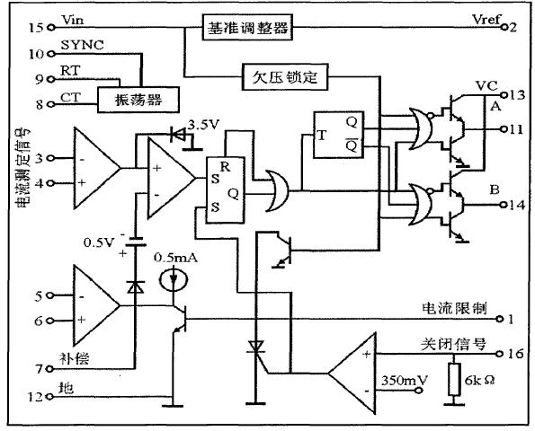
Figure: UC3846 Internal Structure Block Diagram
Soft Start Circuit
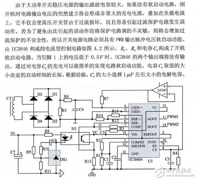
Figure: UC3846 Control Circuit Diagram
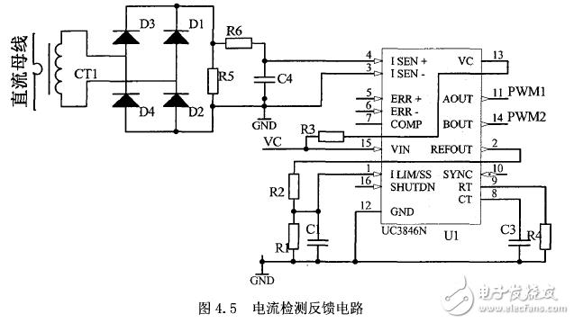
Current Sampling and Voltage Sampling Circuit
In high-power applications, current transformers are commonly used for current detection due to their ability to improve efficiency and provide electrical isolation. This paper utilizes a current transformer to detect the primary current, as shown in the diagram. The use of current transformers ensures accurate monitoring while maintaining safety and efficiency in the system.
Voltage Sampling Circuit
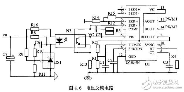
To ensure stable output voltage under varying load conditions, the switching power supply employs an external voltage feedback loop composed of a precision voltage regulator (TL431) and a photocoupler (PC817). The TL431 provides a stable reference voltage that can be adjusted between 2.5V and 36V using external resistors. To achieve isolation between the power ground and output ground, a high-linearity optocoupler is used, ensuring reliable signal transmission without electrical interference.
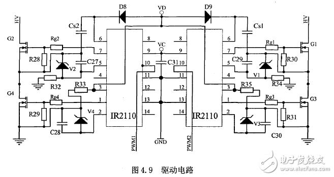
Drive Circuit
The drive circuit serves as a critical interface between the control circuit and the main power circuit. In high-voltage systems, it is essential to isolate the control circuit from the main circuit to ensure safety and proper operation. Two common isolation methods are transformer-based and optocoupler-based isolation. Transformer isolation offers low delay but may suffer from saturation when handling wide pulses. Optocoupler isolation, on the other hand, provides better waveform quality but requires an independent power supply. This design uses the IR2110 optocoupler driver, which features a bootstrap boost circuit for isolation. This configuration improves system stability, reduces size, and enhances speed, making it ideal for high-performance applications.
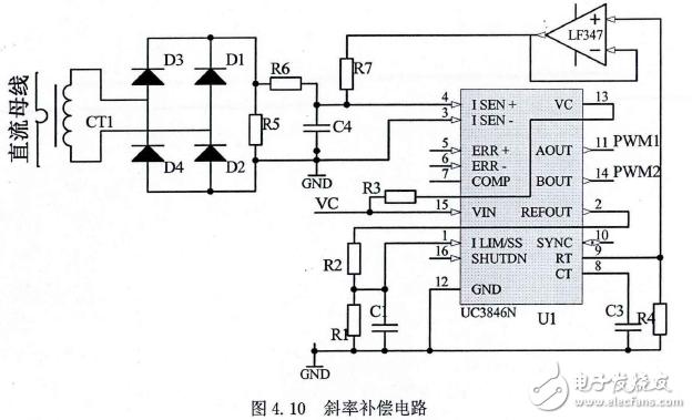
Slope Compensation Circuit Design
Slope compensation is essential to prevent subharmonic oscillations in certain switching topologies. There are two primary approaches: one involves adding the slope compensation signal to the inverting input of the error amplifier, while the other applies the signal to the non-inverting input of the current amplifier. This paper adopts the latter method, incorporating a voltage follower at the non-inverting input of the oscillator and current amplifier. This setup minimizes the impact of current feedback on the oscillation circuit and enhances noise immunity, resulting in a more stable and reliable system.
Auxiliary Power Supply Circuit Design
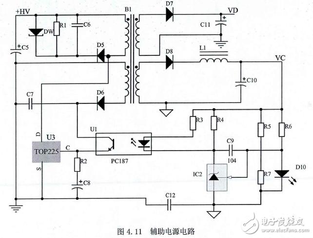
The auxiliary power supply in this design is implemented using a flyback topology based on the three-terminal integrated device TOP225. As shown in the figure, the auxiliary power supply is configured to provide two separate outputs, both at 15V. One output (VC) powers the control and anti-surge protection circuits, while the other (VD) supplies the drive circuit. An RCD snubber circuit, consisting of resistor R1, diode D5, and capacitor C6, is used to suppress voltage spikes that occur during switch turn-off, enhancing the reliability of the system.
Connects PC or laptop with the projector, LCD monitor, and other video display system through VGA connections
Fully shielded VGA / SVGA extension or replacement cable
Supports resolutions at 800x600 (SVGA), 1024x768 (XGA), 1600x1200 (UXGA), 1080p (Full HD), 1920x1200 (WUXGA), and up for high resolution LCD and LED monitors
Gold-plated connectors; 100% bare copper conductors
Each SVGA Cable have two high density HD15 connectors with thumbscrews
Camera Cable,Camera Usb Cable,Usb Camera Adapter,Camera Link Cable
UCOAX , https://www.ucoax.com