1 Introduction to wireless broadband communication
Since the IEEE802 working group formulated the 802-11 wireless local area network standard in 1997, wireless broadband communication based on WLAN technology has developed rapidly. In just six years of development, WI. AN technology continues to develop and mature, and has successively launched 802. ] lb / a / g agreement. The wireless local area network based on the 802.11b protocol works in the 2.4 GHz frequency band and uses CCK modulation technology. The highest data transmission rate can reach 1] Mbps. The wireless local area network based on the 802.1la protocol works in the 5GHz frequency band and uses OFDM modulation technology. The data transmission rate can be as high as 54Mbps. The 802.116 protocol combines the advantages of 802.1h and 801.1b, works in the 2.4GHz band, uses OFDM modulation technology, and has the same rate as the 802.1la standard. In order to solve the problem of compatibility among three communication devices; the same standard wireless network. Several companies have now provided IEEE802.11a / b / g dual-band multi-mode solutions. The standards of 802.11e and 802.1¨ will be released soon. These two standards will separately solve the two outstanding problems on WI: QoS and network security. Intel has successfully applied Centrino technology to notebooks, and people can easily access the wireless broadband through WLAN technology. However, people's application of WLAN technology is not limited to the wireless networking of general-purpose PCs or notebooks. The integration of WLAN technology in embedded systems to achieve wireless broadband communication has become a hot spot for future applications. Examples include home wireless networks composed of wireless digital set-top boxes, computers, wireless gateways, embedded handheld mobile terminals, and industrial control field wireless devices. In recent years, the performance of embedded microprocessors has been greatly improved. Wireless broadband communication modules based on embedded systems can not only realize data transmission, but also meet people's demand for multimedia communication. Here, a microprocessor S3C2410X based on the ARM920T core is used to build an embedded system to complete the function of wireless broadband communication. 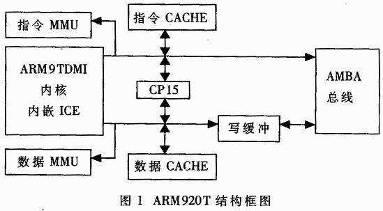
2 S3C2410X embedded processor
S3C2410 is a 16 / 32-bit RISC · embedded microprocessor based on ARM9201 'kernel recently launched by South Korea's Samsung Electronics. The processor is mainly for handheld devices and high cost-effective, low-power applications. Figure 1 is a block diagram of ABNl920T, and Figure 2 is a functional block diagram of S3C2410X integrated resources outside the core [1].
The ARM920T core is composed of three parts: ARM9TDMI, storage management unit MMU and cache. Among them, MMU can manage virtual memory, the cache consists of independent 16KB address and 16KB data high-speed cache. ARM920T has two internal coprocessors: CPl4 and CPl5. CPl4 is used for debugging control, CPl5 is used for storage system control and test control. S3C2410X integrates an LCD controller (supports STN and TFT LCD with touch screen), SDRAM controller, 3 channels of UABT, 4 channels of DMA, 4 timers with PWM function and an internal clock, 10-channel ADC with 8 channels. S3C2410 also has many rich external interfaces, such as touch screen interface, 12 (2 bus interface, male bus interface, two USB host interfaces, one USB device interface, two SPI interfaces, SD interface and MMC card interface. S3C2410X in terms of clock It also has outstanding features. The chip integrates an RTC with calendar function and a chip clock generator with PLL (MPLL and UPLL). MPLL generates the main clock, which can make the processor operating frequency up to 203MHz. The device easily runs WinCE, Linux and other operating systems and performs more complex information processing. UPLL generates a clock that implements the master-slave USB function.
S3C2410X divides the storage space of the system into 8 banks, the size of each bank is 128M bytes, a total of 1G bytes. The start addresses of bsnk0 to bank5 are fixed and used for ROM or SRAM. Bank6 and bank7 are used for ROM, SRAM or SDRAM. These two banks are programmable and the same size. The start address of bank7 is the end address of bank6, which is flexible. The access cycle of all memory blocks is programmable, and the external Wait extends the access cycle. S3C2410X uses nGCS [7: 0] 8 universal chip select lines to select 8 bank areas.
S3C2410X supports NAND flash boot 10ad. NAND flash has the characteristics of large capacity and more competitive price than NOR flash. The system uses a combination of NAND flash and SDRAM to obtain a very high cost performance. The S3C2410X has three boot modes, selected by the OM [l: 0] pins: the processor boots from NAND flash memory at 00; the 16-bit wide ROM bOOt at 01; and the 32-bit wide ROM at 10. The user places the boofload code and operating system image on the external NAND flash memory and uses NAND flash boot. When the processor is powered on and reset, the bootload code is automatically loaded into the internal 4KB SRAM (at this time, the SRAM is located in the starting address space 0x00000000) through the built-in NAND flash access control interface and runs. The boodoad program running in the boot SRAM will operate The image of the system is loaded into SDRAM, and then the operating system can run on SDRAM. After booting, 4KB boot SRAM can be used for other purposes. If booting from other methods, the boot ROM should be located in the starting address space of Ox00000000, the processor directly runs the boot program on the ROM, and the 4KB boot SRAM is located at the memory address 0x40000000.
S3C24lOX uses an independent power supply for each component on the chip: the core uses 1.8V power supply; the storage unit uses 3.3V independent power supply, for general $ DRAbl can use 3.3V, for mobile SDRAM can use VDD equal to 1. /2.5V, VDDQ is equal to 3.0 / 3.3V; I / O uses independent 3.3V power supply [1].
figure 2
3 System hardware platform
Using S3C2410X's excellent core performance and rich external interfaces to construct an embedded system platform for embedded wireless broadband communications. Figure 3 is a hardware block diagram of the system.
In this embedded hardware platform, the main CPU is S3C2410X of SAMSUNG company. The NAND flash memory used as the boot is the SmartMedia card of SAMSUNG. According to the demand for capacity in the application, K9S1208VOM can be selected with a capacity of 64MB, or K9D1G08 with a capacity of 128MB.
SmartMedia cards provide a fairly high price-performance ratio for large-capacity solid-state storage. It is automatically programmed according to pages, each page size is 528 bytes, the typical time of programming is 2001. ts; erasure is carried out in blocks, the size of each block is 16K bytes, the typical erasure time is 2ms. It takes 50ns to read a single data in the page. The SmartMedia card only has 22 pins, 8 I / O lines, read / write control lines and power lines. I / 0 port is a multiplex port for address, command input and data output input. The SmanMedia card also provides ECC error correction codes, realizing bad area detection and real-time mapping, so that it has a program / erase cycle of up to 100,000 times and data storage for up to 10 years. S3C2410X has a dedicated NAND flash interface, so the SmartMedia card is directly connected to this interface on the hardware. In this platform, SmartMedia cards can be used to load operating system images and large-capacity data storage.
SDRAM is used to run the operating system and various types of data cache, which can be used by Samsung, Hyundai and other manufacturers. The K4S561632C from SAMSUNG is used here, which is a synchronous DRAM of 4Mx16bitx4bank with a capacity of 32MB. With 2 K4S561632C, to achieve bit expansion, the data bus width is 32bit, the total capacity is 64MB, its address space is mapped in bank6 of S3C2410.
NOR FLASH uses AMD's AM29LV800B with a capacity of 1MB. Its working voltage can be between 2.7V and 3.6V, the access time is 70ns, and it can be used as boot RON [Flash. The difference with other Flash is that it has a flexible page structure, a 16K byte page, two 8K byte pages, a 32K byte page and L5 64K byte pages. As for its read, write and erase operations, it is no different from general linear flash memory. Here AMD flash memory is mainly used for pre-debugging and operating system download. 
Because S3C2410X itself does not have a PCMCIA interface, in order to connect to the wireless network card of the PCMCIA interface, a dedicated chip must be used as a switch. Here, the [SA-TO-PC-Card controller--PD6710 produced by Intel Corporation is used. PD6710 can control a PC-Card slot, compatible with PC card standard, PCMCDk2.1 and JEIDA4,1. PD6710 uses effective power and mixed voltage technology to reduce the power consumption of the system. At the same time, the chip has a soft control suspend mode and hardware super suspend mode to achieve low power control. The chip uses 82365SL compatible register set, with 5 programmable storage areas and two programmable I / O areas. The connection end of PD6710 and S3C2410X adopts 8-bit or 16-bit ISA-like system bus (here 16-bit system bus), and the connection end of the wireless network card adopts 8-bit or 16-bit PC card bus interface. The wireless network card is the 802.11b standard, which is the most widely used, and the products of major companies provide ready-made drivers. With the widespread use of USB interfaces, there are already wireless network cards with USB interfaces in the city. The S3C2410X integrates a USB host interface and can be directly connected to a wireless network card with a USB interface. If you want to use a wireless card with a CF card interface, you only need to find a CF-PCMCIA adapter to complete the transfer.
In this platform, the CS8900 network card chip is used to connect to Ethernet. The FPGA uses Xilinx's SpartanXL series products. According to functional requirements, the XCS40XL model can be selected to make the number of available doors up to 40K. Using the RAM in SpartanXL series devices can realize high-speed FIFO or use its flexible programmability, which can be used as a general interface between this platform and other external functional modules. For example, when you need to process multimedia data, you can add a DSP to complete, so that S3C2410X can achieve high-speed FIFO and DSP data exchange through FPGA.
As for the design of the human-machine interface, the author uses the 3.5-inch TFT LCD of SAMSUNG company with a touch screen. The input uses the soft keyboard commonly used in PDA.
4 Software platform and system development
S3C2410X integrates a memory management unit, so it can be embedded in a variety of mainstream operating systems, including Windo ~ 's CE, Linux, VxWorks, etc. In this system, Windows CE embedded operating system is selected. For application developers already familiar with the Windows environment, WindowsCE provides a friendly and familiar development environment? Such as Microsoft Win32APl, ActIveX control, message queue, COM interface, ATL and MFC, and there are many successful Windows programs that can be ported to Windows Going to CE greatly improves the efficiency of development. Windows CE embedded operating system can provide users with a familiar and convenient GUI.
The WinCE development platform consists of two parts: Platform Builder and software development kit SDK (Embedded Visual C ++ and Embedded Vi-susl Basic). Platform Builder is used to customize the operating system, and SDK is used to develop applications. The whole Windows CE system is composed of three parts: application program, various components of WinCE and OEM layer. OEM layer interface includes OEM adaptation layer, local driver and stream interface driver. The steps for customizing the operating system are as follows: (1) Write the board-based support package BSP (including OEM adaptation layer OAL and hardware driver); (2) Cut and configure each component of the operating system, and modify the corresponding configuration file; (3) Compile Kemal, components, and BSP to generate an operating system image file; (4) Download the image file to the target device for debugging. After customizing the operating system, export the SDK in the PlatformBuffder to develop applications for the platform in the EmbeddedVisualC ++ or EmbeddedVisualBasic environment [2]. 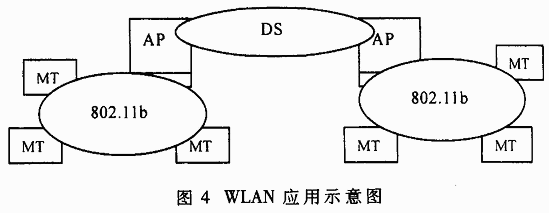
After the operating system is customized, it must be downloaded to the target device. Common methods are as follows: download via JTAC interface, EBOOT download, USB download, serial port download. The latter three download methods must first download the corresponding monitoring program to nash through the JTAC interface, and then the CPU starts from Flash. Because the S3C2410X integrates a slave USB interface, downloading via USB is particularly convenient without Ethernet, and the download speed is much faster than serial download. In actual system development, the JTAC debugger is used to program the USB monitor program to AMD flash memory, and then the S3C2410X is booted from AMD flash memory. The host runs the DNW program provided by SAMSUNG, uses the serial port for information interaction, downloads the BootLoader and the operating system image to SDRAM through USB, and then downloads a NAND flash memory writing program to SDRAM through USB and runs it to bootloader in SDRAM
The system image is written to the SmartMedia card. After the download is complete, change the boot method to allow the S3C2410X to boot from the SmartMedia card, and the operating system can run on the platform.
Once the operating system is loaded, you can install the driver and corresponding application of the wireless network card through Microsoft AcTIveSvnc. In order to avoid reinstalling the wireless network card driver after power failure, the driver can be packaged directly in the operating system. In order to avoid resetting the IP address every time the computer is turned on, a block device is used for permanent registry storage. In the specific implementation, WinCE provides RegCop), the File function saves the registry information and the RegRestoreFile function loads the registry information. If there is a DHCP server in a wireless broadband network, this embedded system can dynamically obtain an IP address through DHCP, which solves the problem of setting an IP address without a human-machine interface because WinCE integrates TCP / IP Protocol! So directly use the Socket interface provided by the operating system to develop various wireless network applications [3].
5 Application
The wireless broadband communication module based on S3C2410X can be widely applied to various mobile terminals in the WLAN network to realize the transmission of data and multimedia. Figure 4 is a schematic diagram of the application of this module in WLAN. AP is a wireless access point, and MT is an on-site wireless communication mobile terminal based on S3C2410X, and wireless communication is carried out between them through 802.11b- ~ y. DS is a distributed system through which APs communicate. Generally, the AP is connected to the wired network, so that the MT can not only communicate with each other, but also realize data transmission with the wired network.
This embedded module integrates rich interfaces, which can not only realize the seamless connection of the wired network and the wireless network, but also realize the wireless monitoring of the image if a CCD camera and a DSP processing module are added. At present, this module has been used in fieldbus wireless communication.
Glue Drying Machine,Automatic Glue Dryer Machine,Manual Glue Drying Machine,Automatic Glue Drying Machine
Zhijiang BSL battery technology service company , https://www.bslbatteryservice.com