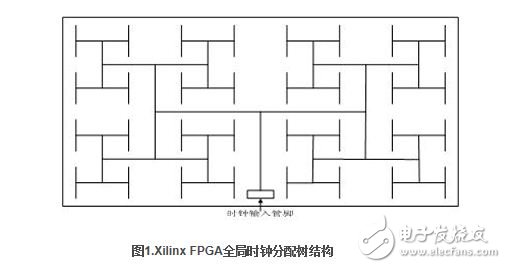
In the Xilinx family of FPGA products, the global clock network is a global routing resource that ensures that the clock signal reaches the same target logical unit with the same latency. Its clock distribution tree structure is shown in Figure 1.
For different types of devices, the global clock network provided by Xilinx is slightly different in terms of quantity and performance. The Virtex-4 series chip is taken as an example to briefly introduce the global clock network structure of the FPGA.
Virtex-4 series FPGAs are fabricated using 1.2V, 90nm triple-gate oxide technology. Flexible clock solutions compared to previous generations, up to 80 independent clocks and 20 digital clock managers, globally differential Clock control technology minimizes skew and jitter. The global clock network implemented in the all-copper process, plus a dedicated clock buffer and driver structure, allows the global clock to reach all logic configurable cells inside the chip, and the I/O cell and block RAM have minimal delay and jitter. Meet the demanding requirements of high-speed sync circuits for clock-triggered edges.
In FPGA design, the FPGA global clock path requires dedicated clock buffering and driving with minimal offset and maximum fan-out capability, so the best clocking scheme is a single master clock driven by a dedicated global clock input pin. Control each trigger in the design project. Whenever possible, global clocks should be used in design projects because the global clock is the simplest and most predictable clock for a design project.
In the software code, the global clock can be used by calling the primitive IBUFGP. The basic usage of IBUFGP is:
IBUFGP U1(.I(clk_in), .O(clk_out));
The global clock network has a great impact on the performance of FPGA design, so this book will introduce the global clock network and related methods in Chapter 11 in more depth and comprehensive.
Use of DCM modules
1. Introduction to the composition and function of the DCM module
The Digital Clock Manager (DCM) is a Digital Delay Phase-Locked Loop (DLL) module based on other Xilinx devices. In terms of clock management and control, DCM is more powerful and flexible than DLL. The functions of the DCM include system requirements such as elimination of clock delay, frequency synthesis, and clock phase adjustment. The main advantages of DCM are:
(1) Implement zero clock offset (Skew), eliminate clock distribution delay, and implement clock closed-loop control;
(2) The clock can be mapped to the PCB for synchronizing the external chip, thus reducing the requirement for the external chip and integrating the clock control inside and outside the chip to facilitate system design. For the DCM module, the key parameters are the input clock frequency range, the output clock frequency range, and the input/output clock allowable jitter range.
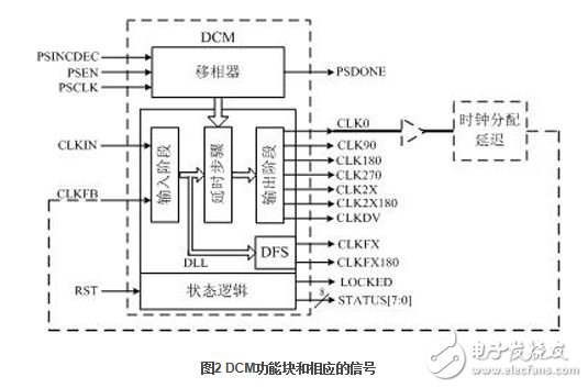
The DCM consists of four parts, as shown in Figure 2. The bottom layer still uses mature DLL modules; secondly, digital frequency synthesizer (DFS), digital phase shifter (DPS, Digital Phase Shifter) and digital spectrum spreader (DSS, Digital Spread Spectrum). The DCM input frequency range of different chip modules is different, for example:
1) DLL module
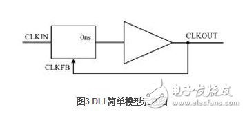
The DLL consists primarily of a delay line and control logic. The delay line generates a delay to the clock input CLKIN. The clock distribution network line distributes the clock to each register in the device and the clock feedback terminal CLKFB. The control logic samples the input clock to adjust the deviation between the two when the feedback clock arrives. , to achieve zero delay of input and output, as shown in Figure 3. The specific working principle is: after comparing the deviation between the input clock and the feedback clock, the control logic adjusts the delay line parameters, and inserts the delay after the input clock until the input clock and the rising edge of the feedback clock are synchronized, and the locking loop enters. In the "locked" state, the input clock and feedback clock are synchronized as long as the input clock does not change. DLLs can be used to implement circuits to refine and simplify system-level design, such as providing zero propagation delay, low clock phase difference, and advanced clock region control.
In the Xilinx chip, the typical DLL standard prototype is shown in Figure 4. The pins are described as follows:
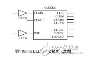
CLKIN (Source Clock Input): DLL input clock signal, usually from IBUFG or BUFG.
CLKFB (Feedback Clock Input): DLL clock feedback signal, which must be derived from CLK0 or CLK2X and connected via IBUFG or BUFG.
RST (Reset): Controls the initialization of the DLL, usually grounded.
CLK0 (same frequency signal output): no phase offset from CLKIN; CLK90 has a 90 degree phase offset from CLKIN; CLK180 has a 180 degree phase offset from CLKIN; CLK270 has a 270 degree phase offset from CL KIN.
CLKDV (divided output): DLL output clock signal, which is the divided clock signal of CLKIN. The DLL supports a division factor of 1.5, 2, 2.5, 3, 4, 5, 8, and 16.
CLK2X (twice signal output): 2 times the clock signal of CLKIN.
LOCKED (output latch): In order to complete the latch, the DLL may have to detect thousands of clock cycles. LOCKED is valid when the DLL has finished latching.
- Wall Socket Expansion allowing you to expand one in wall socket to multi outlets, as well as to add more functions, e.g. socket plus USB ports, or with surge protector, or with overload protection.
- Multiple Outlets allowing you to plug in multiple electrical devices.
- Compact Wall Expansion is also convenience as travel power adapter from its weight and size point of view.
- PC/ABS flame retardant, phosphor bronze+pure copper.
- Space saving and cost saving
- We have been doing OEM service for Germany customer since the very beginning time when we started power strip manufacturing.
Now we still continue with OEM/ODM services and doing our own design as well.
- Own factory
Wall Socket Expansion
Wall Socket Expansion, Compact Wall Expansion, USB Wall Socket, Multi Outlets Wall Socket
ZhongShan JITONGLONG Plastic Hardware Co. Ltd. , https://www.toukoo-electronics.com