In the analog-to-digital converter (ADC) circuit design, especially when the system designer needs to handle the voltage signals of various swings, it is easy to generate a misunderstanding to narrow the input signal range to fit the full-scale range of the ADC. The signal-to-noise ratio (SNR) will be greatly reduced. Taken together, the choice of low voltage (5V or lower) ADCs is wider than for high voltage ADCs. High supply voltages typically result in large power dissipation and board design is more complex, for example, requiring more decoupling capacitors. This application note discusses SNR loss due to signal reduction, how to quantify these losses, and how to reduce these losses.
Many sensor or system outputs are high voltage or bipolar consumption, such as the common ±10V. Of course, these signals can be sent to the ADC in a few simple ways to process these wide-range input signals with high-voltage ADCs without SNR loss. These solutions typically require additional high voltage power to meet the input range and higher power requirements (Figure 1). These high voltage ADCs also limit the use of signal conditioning (op amp) solutions. If the signal requires multiplexing of high voltage and low voltage inputs, the actual circuit cost will be higher (Figure 2).
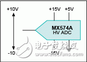
Figure 1. The MX574A high voltage ADC can support a large input signal range, but also consumes higher power.
In order to achieve this solution, it must be powered by a ±15V dual supply and a +5V single supply.
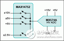
Figure 2. Multiplexed, bipolar high voltage input ADC system.
An input op amp can also be used to reduce the signal to the full-scale range of the low-voltage ADC. The signal conditioning circuit can be connected to a separate analog switch input (Figure 3) to limit all signals to the ADC input range.
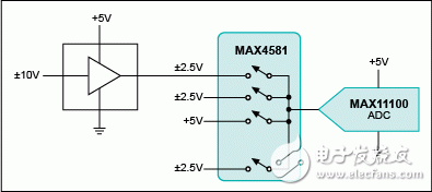
Figure 3. Processing a high-voltage input with a single MAX11100 low-voltage ADC and multiplexer.
When the op amp is used to reduce the signal voltage range, the op amp noise can be equivalent to the op amp's input noise. There are two main noise sources here: the op amp reference input noise and the ADC input reference noise generated by the compressed signal. These two noise sources are combined into a quadratic equation. In addition, the amplifier noise is filtered through the ADC input bandwidth and the anti-aliasing filter between the op amp and the ADC input, as shown in Figure 4.
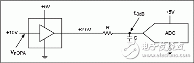
Figure 4. The proportional op amp introduces noise, but the noise is filtered by the RC filter and the ADC input network.
The system SNR (op amp input front end) formula is:
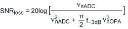
among them:
![]() nADC = ADC's input RMS noise
nADC = ADC's input RMS noise
![]() nOPA = op amp input noise
nOPA = op amp input noise
f-3dB = single pole point -3dB frequency
For a given ADC full-scale range, ADC input reference noise, and op amp gain, there are two parameters that affect the final SNR loss: filter cutoff frequency and amplifier input reference noise.
If the signal source has a low frequency component, it can be designed to have a higher input noise margin (which guarantees low power consumption and low cost while sacrificing certain noise performance). If the ADC limits the system bandwidth, the op amp is required to have low enough input noise to meet the SNR requirement.
As an example, the input signal is ±10V, while the ADC full-scale input is 5VP-P and the ADC SNR is 92dB. At this point, the amplifier's attenuation factor is 4 times (adjust the input to full scale). The ADC input noise provided in the data sheet is 44.4nVRMS. Assuming a filter cutoff frequency of 10 kHz, if an op amp with an input noise of 10 nV/√Hz is used, the loss signal-to-noise ratio is:
SNR(loss) = 0.035dB
If the filter is not used, the ADC bandwidth is 10MHz. In order to control the SNR to the same level, the input noise is required to be 0.3nV/√Hz, which is difficult to achieve in the design.
For an ADC with the same 10MHz bandwidth, if we allow SNR(loss) = 0.5dB, the op amp noise specification is required to be 4nV/√Hz, which is easy to do.
Featuring level VI energy efficiency and meet international safety standards, the external ac to dc Power Adapter accepts universal AC input voltage ranging from 100V to 240V and provides 3 years warranty. These wall plug series power adapters includes safety protections for over voltage, over current and short circuit.
5V Dc Adapter,Travel Plug Adapter,Ul Power Adapter,Wall Plug Power Supply,Adapter 230V 24V
Shenzhenshi Zhenhuan Electronic Co Ltd , https://www.szzhpower.com