This section will briefly describe how to use the ChipScope core and analysis tools for logic debugging and verification in the PlanAhead tool. First insert a ChipScope core into the design through a wizard, select the network cable to be tested, instantiate, connect and synthesize. Finally, import the layout and timing report, generate a bitstream file, and verify with the ChipScope analyzer.
1. Open the project.(1) Run PlanAhead, find the project "Project_cpu_hdl.ppr" in the directory "PlanAhead_Tutorial\Projects\project_cpu_hdl" and open it. The PlanAhead window is displayed as shown in Figure 10-86.
![[PlanAhead] window](http://i.bosscdn.com/blog/06/33/0E/A4_0.png)
Figure 10-86 [PlanAhead] window
(2) Store the project as another project to ensure that the original project is not damaged. Run [File] → [Save Project as] to open the [Save Project As] dialog box and set the project name and project storage path as shown in Figure 10-87.
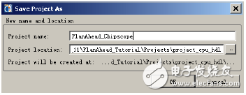
Figure 10-87 Setting the project name and storage path
2. Apply the [Set Up ChipScope] wizard.(1) [Set Up ChipScope] The wizard guides the designer to insert ChipScope's ICON core and ILA core into the integrated netlist, select the network cable to be tested, set the number of inserted ChipScope cores, and then instantiate these cores. Select the network cable and the core to connect.
(2) Run the [Tools] → [Set Up ChipScope] wizard to connect the wbArbEngine/m0/wb* network cable to the ChipScope core. As shown in Figure 10-88.
![[Set Up ChipScope] window](http://i.bosscdn.com/blog/06/32/11/2609_0.png)
Figure 10-88 [Set Up ChipScope] Window
(3) Click [Next], and the [Specify Nets to Debug] window shown in Figure 10-89 appears.
![[Specify Nets to Debug] dialog box](http://i.bosscdn.com/blog/06/32/0c/R2_0.png)
Figure 10-89 [Specify Nets to Debug] Dialog Box
(4) Click the [Add/Remove Nets] button, and the [Add/Remove Nets] dialog box shown in Figure 10-90 appears. Find the matching condition as wbArbEngine/m0/wb_* according to the settings shown in the figure, and click [Find] 】 button, the search results will be displayed in [Find Results].
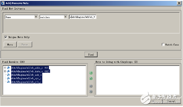
Figure 10-90 Finding results
(5) Click the button to select the discovered network cable as the network to be tested, as shown in Figure 10-91. Click [OK] to exit the network cable setting dialog box.
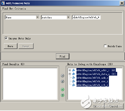
Figure 10-91 Adding a network cable to be tested
(6) Click [OK] to exit the network cable setting dialog box. At this time, the [Specify Nets to Debug] dialog box is displayed as shown in Figure 10-92. It can be seen that a total of 39 network cables to be tested are added. Click the [Next] button, the [Set Up ChipScope Summary] dialog box appears, click [Finish], in the [Netlist] window of PlanAhead, you can see that csdebugcore_0_0, csdebugcore_0_1 and u_icon have been added after adding the ChipScope core, as shown in Figure 10- 93 shows.
![[Specify Nets to Debug] dialog box after adding a network cable](http://i.bosscdn.com/blog/06/29/34/4492_0.png)
Figure 10-92 [Specify Nets to Debug] dialog box after adding a network cable
![Added [Netlist] window of ChipScope core](http://i.bosscdn.com/blog/06/30/02/93W_0.png)
Figure 10-93 Adding the [Netlist] window of the ChipScope core
3. Modify the properties of the ChipScope core and trigger signal.As shown in Figure 10-94, select a set of trigger signal TRIG0 in the [ChipScope] view, and select the [OpTIons] tab in [Debug Port ProperTIes] to change the match_type attribute and select different trigger conditions.
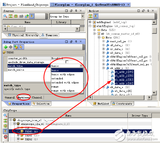
Figure 10-94 Changing the trigger attribute
As shown in Figure 10-95, select ChipScope's ILA core in the [ChipScope] view, and select the [OpTIons] tab in [Debug Core ProperTIes], where you can modify the properties of the core, such as the sampling depth and the sampling clock edge.
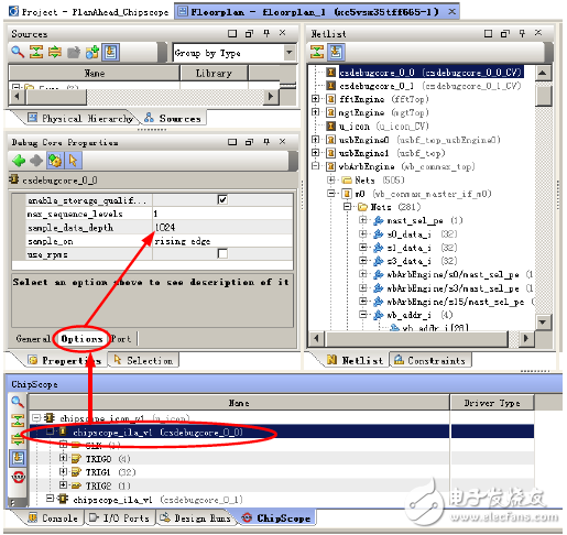
Figure 10-95 Changing the ChipScope Core Attribute
4. Implement the ChipScope core.In the [ChipScope] window shown in Figure 10-96, select an ILA core and click the button to implement the ChipScope Debug Cores. This command calls the COREGen tool to convert the black box ChipScope debug core into a comprehensive ChipScope core. It can then be translated, mapped, laid out.
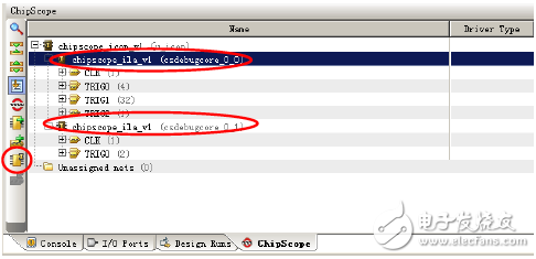
Figure 10-96 Implementing the ChipScope Core
In addition, the reader can select an ILA core in the [ChipScope] window, right-click and select [Schematic], you can see the schematic module of the ChipScope core, as shown in Figure 10-97.
![[Schematic] window](http://i.bosscdn.com/blog/06/2S/1Q/26_0.png)
Figure 10-97 [Schematic] Window
Lithium-boron alloy is a composite material composed of a brittle Li7B6 matrix phase with a porous structure and a ductile Li filling phase. The density is 0.88±0.04g/cm3. The appearance is silver-white metal. It is extremely unstable. It is easily deteriorated when exposed to air and reacts with water. severe. Lithium-boron alloy is mainly used as anode material for lithium-based thermal batteries. It has outstanding advantages such as high specific energy, high specific power and low polarization, electrochemical potential similar to that of pure lithium, and solid state above 600℃. It is a new type of lithium-based thermal battery. The excellent negative electrode material. Compared with the currently widely used Lithium-Silicon Alloy, the unit cell assembled with the lithium-boron alloy as the negative electrode material has better performance in both the highest voltage and the discharge working time.
Shandong Huachuang Times Optoelectronics Technology Co., Ltd. , https://www.dadncell.com