Under the guidance of Moore's Law, the manufacturing process of integrated circuits has been evolving. Proud of the popularity of smartphones over the past few years, everyone knows a lot about nodes. For example 40nm, 28nm, 20nm, 16nm, etc., but do you know the true meaning of these nodes? Do you know how they evolved? Let's take a look at this report.
First, let's analyze what the technical node means.
Often heard, such as TSMC 16nm Nvidia GPU, Intel 14nm i5, etc., the meaning of this length, the specific definition needs to give a detailed structural diagram of the transistor, simply, in the early days At that time, it can be considered as equivalent to the size of the transistor.
Why is this size important? Because of the action of the transistor, simply speaking, electrons are sent from one end (S) through a channel to the other end (D). After the process is completed, the transfer of information is completed. Because the speed of electrons is limited, in modern transistors, it is generally operated at saturation speed, so the time required is basically determined by the length of this channel. The shorter, the faster. The length of this channel, and the size of the transistor previously described, can generally be considered to be uniform. But there is a difference between the two, the channel length is a transistor physical concept, and the size used for the technology node is the concept of the manufacturing process, the two are related, but not equal.
In the micron era, the smaller the number of this technology node is, the smaller the transistor size is, and the smaller the channel length is. But after the 22nm node, the actual size of the transistor, or the actual length of the channel, is longer than this number. For example, Intel's 14nm transistor, the channel length is actually about 20nm.
According to the current understanding, there are three problems involved in the shrinking process of transistors, namely:
First, why should we reduce the size of the transistor? And what is the scale of the reduction? The question is asking, what are the benefits of narrowing down?
Second, why is the number of technology nodes not equal to the actual size of the transistor? Or, in the case where the actual size of the transistor is not scaled down, why is it claimed to be a new generation of technology nodes? This question is asking, what technical difficulties are there to narrow down?
Third, how to narrow down? That is, what is the development history of technology nodes? What kind of technological progress is there in every generation? This is also the real question raised by the subject. I refer specifically to the design and materials of transistors here, as explained above.
Please do my best to answer below, please correct me. 
Why shrink the transistor size?
The first problem is that the smaller the transistor size, the faster the speed. This fast can be directly translated into the performance of transistor-based integrated circuit chips. Let's take the microprocessor CPU as an example. First, the above picture is from 40 Years of Microprocessor Trend Data.
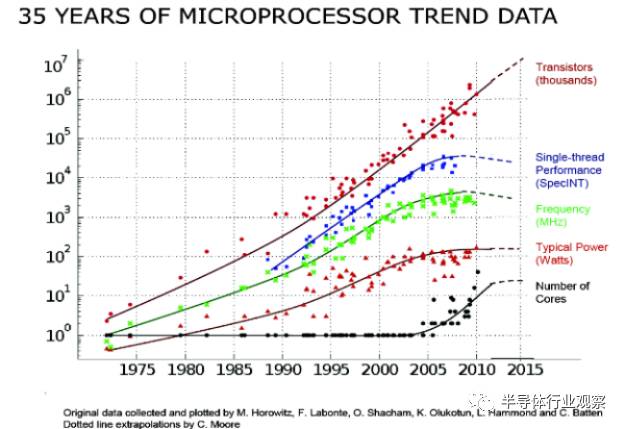
The amount of information in this picture is very large. The relevant point here is the green point, which represents the clock frequency of the CPU. The higher the frequency, of course. It can be seen that until about 2004, the clock frequency of the CPU is basically exponentially rising, and the main reason behind it is that the size of the transistor is reduced.
Another important reason is that after the size is reduced, the degree of integration (the number of transistors per unit area) is increased, which has several advantages, which can increase the function of the chip, and more importantly, according to Moore's Law, the integration is improved. The direct result is a drop in cost. That's why the semiconductor industry has been pursuing Moore's Law for 50 years, because if you don't meet this standard, your family's product cost will be higher than the opponents who can reach this standard, and your family will go bankrupt.
Another reason is that transistor shrinking can reduce the power consumption of a single transistor because of the reduced regulatory requirements, while reducing the overall chip supply voltage, which in turn reduces power consumption.
But one important exception is that physical power consumption does not decrease per unit area. Therefore, this becomes a very serious problem of transistor shrinkage, because the theoretical calculation is an ideal situation. In fact, not only does it not decrease, but it increases with the increase of integration. At around 2000, people have predicted that according to the development of Moore's Law, if there is no technological advancement, when the transistor shrinks to around 2010, the power density can reach the level of the rocket engine. Such a chip is of course impossible to work properly. of. Even if this level is not reached, too high a temperature will affect the performance of the transistor.
In fact, the industry has not found a solution to completely solve the problem of transistor power consumption. The actual method is to reduce the voltage (the power consumption is proportional to the square of the voltage), and no longer pursue the clock frequency. Therefore, in the above figure, after 2005, the CPU frequency will no longer increase, and the performance improvement mainly depends on the multi-core architecture. This is called the "power wall" and still exists today, so you can't buy a 5GHZ processor, and almost no 4G.
These are the main causes of three shrinking transistors. It can be seen that all of them are heavyweight methods of improving performance, function and cost reduction, so the industry will continue to do so until now.
So how is it reduced? The physical principle is a constant electric field, because the physics of a transistor is generally determined by an electric field, so as long as the electric field is constant, the model of the transistor does not need to be changed. This method proves to be the best, called Dennard Scaling, The one is IBM.
The electric field is equal to the voltage divided by the size. Since you want to reduce the size, you have to wait for the voltage to decrease.
How to reduce the size? Simple and rude: It's good to reduce the area to half. The area is equal to the square of the size, so the size is reduced by about 0.7. If you look at the number of transistor technology nodes:
130 nm, 90 nm, 65 nm, 45 nm, 32 nm, 22 nm, 14 nm, 10 nm, 7 nm (5 nm)
It will be found that this is a ratio of approximately 0.7, which is the reason. Of course, as I said before, this is just a naming habit, and there is already a gap between the actual size and the actual size.
Why is the number of nodes not equal to the actual size of the transistor?
The second question, why does the current technology node no longer directly reflect the size of the transistor?
The reason is also very simple, because this level of reduction can not be achieved. There are three main reasons:
First, the atomic scale is measured in amps, which is 0.1 nm.
With a channel length of 10 nm, there are less than 100 silicon atoms. The physical model of the transistor is such that the distribution of electrons is calculated using the band theory of quantum mechanics, but the transport of electrons is calculated using classical current theory. After the distribution is determined, the electron is still treated as a particle, not its quantum effect. Because it is large in size, it is not needed. But the smaller, the less it is, the more complex physical effects need to be considered, and the current model of the transistor is no longer applicable.
Secondly, using the classic model, there is a problem in performance. This is called short channel effect, and its effect is to damage the performance of the transistor.
The short channel effect is actually well understood. In a nutshell, the transistor is a three-port switch. As mentioned above, the working principle is to take electrons from one end (source end) to the other end (drain end), which is carried out through the channel, and another port (gate end) is used to determine this Whether the channel is open or closed. These operations are done by adding a specific voltage to the port.
One thing that transistor performance relies on is that it must be turned on and tight. Short-channel devices can be opened without problems, but they are not tight. The reason is that the size is too small. There are many internal interferences on the electric field. It used to be negligible. Now the electric field at the gate cannot be used. The role, so the closure is not tight. The consequence of not being tight is that there is leakage current, which is simply a current that is not needed and wasted.
This part of the current can not be underestimated, because the transistor is at rest, does nothing, but consumes power in vain. At present, the energy consumption caused by this part of the leakage current in the integrated circuit has accounted for nearly half of the total energy consumption, so it is also one of the most important goals of transistor design and circuit design.
Finally, the manufacturing process is getting harder and harder to achieve that small size.
The thing that determines the minimum size of the manufacturing process is called a lithography machine. Its function is to wash the pre-printed circuit design onto the surface of the wafer like a photo, which in my opinion is a bug-level existence because the throughput is very high. Otherwise how can a complex integrated circuit be made? For example, Intel's Pentium 4 processor is said to require more than 30 or more than 40 different design templates, and has been continuously exposed to complete the design of the entire processor.
But the lithography machine, as its name suggests, uses light, of course not visible light, but in general it is light.
A little common sense will know that all things that use light have an essential problem, that is, diffraction. The lithography machine is no exception.
Because of this problem, the minimum size that any lithography machine can engrave is roughly proportional to the wavelength of the light source it uses. The smaller the wavelength, the smaller the size. This is very simple.
The current mainstream production process uses a stepper lithography machine produced by Esmore, the Netherlands. The light source used is a 193 nm argon fluoride (ArF) molecular oscillator (this name cannot be remembered) and is used in the most Fine lithography steps.
In contrast, the current smallest mass-produced transistor size is 20nm (14nm node), which is more than 10 times the difference.
Some people ask why there is no diffraction effect? The answer is that the industry has invested heavily in lithography for more than a decade, and has developed various violent techniques at the level of magic, such as immersion lithography (putting the optical path in a liquid because of the refractive index of light) Higher, and the smallest size is inversely proportional to the refractive index), the phase mask (by 180 degrees of reverse way to make the generated diffraction cancel each other out, improve the accuracy), and so on, it can be soothing, so it has been supported until now, supported Advances in all technology nodes since 60nm.
Then someone asked, why not use a light source with a smaller wavelength? The answer is that the process can't be done temporarily.
Yes, the source of high-end lithography is a world-class industrial problem.
The above is the current mainstream deep ultraviolet exposure technology (DUV). The industry generally believes that the 7nm technology node is its limit, and even 7nm is not necessarily capable of mass production. The next generation of technology is still under development, known as extreme ultraviolet (EUV), and its light source has dropped to 13nm. But don't be too happy, because at this wavelength, there is no suitable medium that can be used to refract light, which constitutes the necessary optical path. Therefore, the optical design in this technology is all reflection, and with such high precision, design Such a complex reflected light path is an unimaginable technical problem in itself.
This is not the case (already overcome). The most difficult thing is the light source. Although it can produce the required light, the intensity is much lower than that of industrial production, resulting in the wafer output of the EUV lithography machine not meeting the requirements, in other words. If you use it, you will lose it. One such machine is hundreds of millions of dollars. So EUV is still in the future.
There are three reasons for this. In fact, the size of the transistor has shrunk into the deep water area very early, and it is getting harder and harder. After 22nm, it has not been able to scale up much, so there is no need to narrow down. The use of a more optimized transistor design, coupled with a series of technologies such as multi-core multi-threading on the CPU architecture, continues to provide consumers with the equivalent of updated product performance.
For this reason, the number of technology nodes is still shrinking, but it is no longer equivalent to the size of the transistor, but the sum of the technologies and processes that represent the set of indicators that make up this technology node.
Problems faced during transistor shrinkage
The third question is how the design of the transistor develops during the shrinking of the technology node.
First of all, figure out what the idea of ​​transistor design is. The main thing is nothing more than two points: the first boost switch responsiveness and the second decrease leakage current.
In order to clarify this issue, the best way is to look at the picture. The physical diagram of the transistor is basically enough to figure out one, that is, the leakage current-gate voltage relationship, such as the following:
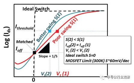
The horizontal axis represents the gate voltage, the vertical axis represents the leakage current, and the vertical axis is generally a logarithmic coordinate.
As mentioned earlier, the gate voltage controls the switching of the transistor. It can be seen that the best transistor is one that can change from a complete turn-off (leakage current is 0) to a full turn-on (leakage current reaches saturation value), that is, a dotted line. . This property has many advantages, and then I will talk about it.
Obviously this transistor does not exist on this planet. The reason is that under the classical transistor physics theory, the standard for measuring the response capability of this switch is called Subthreshold Swing (SS, not the SS...), and there is a limit value of about 60. The reason behind it is not elaborated. It is.
Intel's data, the latest 14nm transistor, this value is about 70 (the lower the better).
Also, lowering this value, and lowering the leakage current, increasing the operating current (increasing the speed), and reducing the power consumption are equivalent, because the lower the value, the lower the leakage current at the same voltage. In order to achieve the same operating current, the lower the required voltage, which is equivalent to reducing power consumption. So this value is the most important indicator in the transistor design, not too much.
What do you do around this indicator and the several goals behind transistor performance design?
Look at industry first, after all, practice is the only criterion for testing truth. The following is my memory, and the correspondence with the nodes is not necessarily completely accurate, but the specific description should be correct:
65 nm introduces the channel of Ge strained.
Strain I don't know how to translate into Chinese vocabulary, but the principle is that by doping a little bit into the silicon in the appropriate place, the lattice constant of germanium and silicon is different, which will cause the lattice shape of silicon to change. According to the band theory, this change can increase the mobility of electrons in the direction of the channel, and the high mobility will increase the operating current of the transistor. In practice, it has been found that this method is more effective for a transistor of a hole type channel (pmos) than a transistor of an electron type channel (nmos).
A breakthrough in milestones, introducing a high-k insulating layer at 45nm
45nm introduces a high-k insulating/metal gate configuration.
This is also a milestone. I used to have a professor who helped him move bricks when I was studying. I was one of the main members of the team that developed this technology in Intel. So I mentioned this very much. Just remember.
These are two technologies, but they are all designed to solve the same problem: how to ensure the effective operation of the gate in a small size.
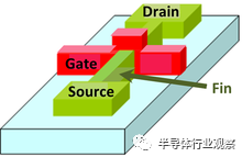
The structure of the transistor is not detailed in the front, and the following picture is added:
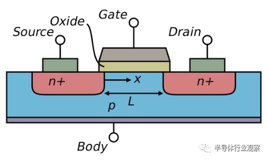
This is a schematic diagram of the most basic transistor. Nowadays, the transistor is not long, but any semiconductor physics starts from here, so this is the "standard version" of the transistor, also known as the body. A bulk transistor.
The gate is the gate.
There is an oxide, insulating layer, not mentioned before, but it is the most critical one of all the components of the transistor. Its role is to isolate the gate and the channel. Because the gate switch channel is made by the electric field, the electric field is generated by adding a certain voltage to the gate, but Ohm's law tells us that there is a voltage and current. If there is current flowing from the gate into the channel, what switches are you talking about? It has long since leaked.
Therefore, an insulating layer is required. Why is it called oxide(or "dielectric") instead of an insulator? Since the earliest insulating layer is silicon dioxide that coexists with silicon very naturally, its relative dielectric constant (the higher the insulation, the better the transistor performance) is about 3.9. A good insulating layer is the lifeline of a transistor. The definition of "good" is not mentioned here, but it should be noted that silicon naturally has such a super-performance insulating layer. For the semiconductor industry, it is one. Lucky things of historical significance. Someone once said that God is helping humans to invent integrated circuits, first giving so much sand (the raw material for silicon wafers) and giving a perfect natural insulation layer. So far, silicon is extremely difficult to replace. An important reason is that the overall performance of the material used to make the transistor is perfect.
Although silica is good, problems have also arisen when the size is reduced to a certain limit. Don't forget that the electric field strength remains constant during the process of shrinking. In this case, from the perspective of the energy band, because of the volatility of the electrons, if the insulating layer is narrow and narrow, then there is a certain probability of electrons. A tunneling effect occurs across the energy barrier of the insulating layer, causing leakage current. Imagine crossing a wall that is taller than yourself. The magnitude of this current is inversely related to the thickness of the insulating layer and the "barrier height" of the insulating layer. Therefore, the smaller the thickness, the lower the barrier, and the larger the leakage current, the more unfavorable the transistor.
But on the other hand, the switching performance, operating current, etc. of the transistor need to have a large insulation layer capacitance. In fact, if this capacitance is infinite, then the idealized 60 SS indicator will be reached. The capacitance mentioned here refers to the capacitance per unit area. This capacitance is equal to the dielectric constant divided by the thickness of the insulating layer. Obviously, the smaller the thickness, the larger the dielectric constant, which is more advantageous for the transistor.
Then it can be seen that there has been a contradiction in a pair of design goals, that is, whether the thickness of the insulation layer should continue to shrink. In fact, before this node, silicon dioxide has been reduced to a thickness of less than two nanometers, that is, the thickness of a dozen atomic layers. The problem of leakage current has replaced the performance problem and became the number one enemy.
So the clever human beings began to think of ways. Human beings are very greedy, neither willing to give up the performance enhancement of large capacitors, and are not willing to risk leakage. So humans say that if there is a material with a high dielectric constant and a high potential barrier, then it is possible to continue to increase the capacitance (improve the switching performance) without reducing the thickness (protecting the leakage current). What?
So everyone started looking for, using almost violent methods, looking for a lot of strange materials, and finally finally verified to use a material called HfO2. I have never heard of this element before, I can't say anything about Chinese. It is such a cow. This is called high-k, where k is the relative dielectric constant (relative to silica).
Of course, the complexity of this process is far more than that described here. There are many materials with high-k properties, but the materials that are ultimately used must have many excellent electrical properties, because silicon dioxide is really a perfect transistor insulation material, and the manufacturing process and integrated circuits. Other manufacturing steps can be easily integrated, so finding such a high-performance insulation material that meets the requirements of semiconductor process manufacturing is an amazing engineering achievement.
As for the metal grid, it is a technology that is compatible with high-k. In the earliest days of the transistor, the gate was made of aluminum, which was later developed to be made of heavily doped polysilicon because of its simple process and good performance. At high-k, we found that high-k materials have two side effects, one will inexplicably reduce the operating current, and the other will change the threshold voltage of the transistor. The threshold voltage is the minimum voltage required to turn the transistor's channel on. This value is a very important transistor parameter.
This principle is not elaborated. The main reason is that the high-k material reduces the carrier mobility in the trench and affects the position of the Fermi level at the interface. The lower the carrier mobility, the lower the operating current, and the so-called Fermi level is an analytical method for interpreting the distribution of semiconductor electrons from the band theory image. Simply put, its position affects the transistor. Threshold voltage. Both of these problems are related to the dipole distribution inside the high-k material. A dipole is a pair of charge systems with a positive charge at one end and a negative charge at one end. It can change its distribution with the direction of the applied electric field. The reason why the dielectric constant of high-k material is high is the internal dipole. There is a big relationship. So this is a double-edged sword.
Then humans thought, they thought of using metal as the gate, because the metal has an effect called image charge, which can neutralize the influence of the dipole in the insulation layer of high-k material on the channel and Fermi level. This will give you the best of both worlds. As for what kind of metal or these metals are, I am sorry that no one outside of the company who knows the technology knows that it is a trade secret.
Then Moore's Law won again.
32nm second generation high-k insulation/metal gate process.
Because 45nm Intel has achieved great success (in the development of many transistors and microprocessors, the 45nm generation of transistors will suddenly appear a big improvement in power consumption, performance, etc.), continue to be based on 32nm Change the better materials and continue the old way of downsizing. Of course, the previous generation Ge strain process is still used.
22nm FinFET (Intel becomes Tri-gate), tri-gate transistor.
This generation of transistors has undergone a revolution in architecture. The earliest design of the change can be traced back to the physical model of the tri-gate and ring-gate transistors proposed by Professor Hu Zhengming of Berkeley in 2000, which was later turned into reality by Intel.
The general model of FinFET is long. It essentially adds a gate.
Why do you do that? Intuitively, if you look back at the previous "standard version" of the transistor structure, in a very short transistor, the leakage current is more serious because of the short channel effect. Most of the leakage current flows through the area below the channel. The channel is not shown on the figure and is a very thin layer of very very thin (one or two nanometers) below the oxide insulating layer, on the surface of the silicon wafer. The area under the channel is called the depletion layer, which is the majority of the blue area.
Smart IBM, genius Intel
Then someone began to think, since the electrons move in the channel, why should I leave such a large depletion layer under the channel? Of course this is for a reason, because the physical model needs this area to balance the charge. However, in a short-channel device, it is not necessary to put the depletion layer and the channel together, waiting for the leakage current to flow freely.
So someone (IBM) opened a brain hole: take this part of the silicon directly and replace it with an insulating layer. Below the insulating layer is the remaining silicon, so that the channel is separated from the depletion layer because the electrons are derived from the two poles. However, the two poles and the depletion layer are separated by an insulating layer, so that there is no leakage other than the channel. For example:
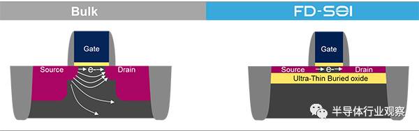
This is called SOI (silicon on insulator), although it has not become mainstream, but because of its advantages, there are still manufacturers.
Then someone (Intel) thought again, since all the silicon in the depletion layer was removed and an oxide layer was inserted, why should we put a bunch of useless silicon underneath, directly under the oxide layer, and then make another The grid, the channel on both sides, isn't it better? You see IBM, you are not ambitious.
But Intel still feels inadequate, and thinks, in this case, what is necessary to bury the oxide layer in silicon? I got the silicon out, wrapped the insulation around the sandwich, and put the grid on the outside. Isn't it cool?

Then there is the FinFET, the above. The FinFET's strength is that it not only greatly reduces the leakage current, but because there is one more gate, the two gates are generally connected together, which is equivalent to greatly increasing the insulation capacitance mentioned earlier. That is, the switching performance of the transistor is greatly improved. So it is a revolutionary progress.
This design is not difficult to think of, the hard part is that it can be done. why? Because the part of the silicon that is erected, that is, the silicon used as the channel, is too thin, less than 10 nanometers, not only much smaller than the minimum size of the transistor, but also much smaller than that of the most sophisticated lithography machine. smallest size. So how to get this Fin out, have to get it, it has become a real problem.
Intel's approach is very clever. It requires a lot of process flow diagrams to explain, not to mention, but the basic principle is that this part of silicon is not lithographic, but grows. It first engraves a bunch of "shelves" with ordinary precision lithography, and then deposits a layer of silicon, which grows a thin layer of silicon at the edge of the shelf, and then selectively etches the excess material with selective etching. Going, the rest is the standing, ultra-thin silicon fin. When I heard about this method, I was completely embarrassed. This IQ is too crowded.
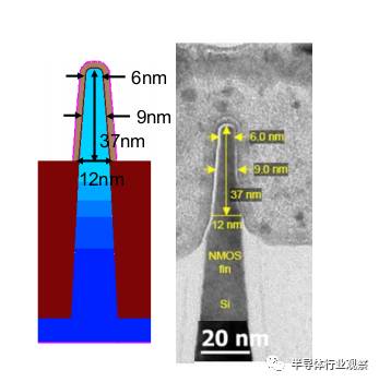
14nm continues the FinFET. Below is a SEM cross-sectional view of Intel's 14nm transistor. As you can see, the width of the fin is only 9nm on average:
Of course, in all the technical nodes of future generations, the technology of the previous generation is also continuously integrated. So now, in the industry and the research community, the transistors that are commonly heard are called high-k/metal gate Ge-strained 14 nm FinFETs, which integrates many years of technical essence.
Struggling for the continuation of Moore's Law
In the academic world, in recent years, various whimsical new designs have been developed, such as tunneling transistors, negative capacitance transistors, carbon nanotubes, and so on.
All of these designs are basically in four directions, materials, mechanisms, processes, and structures. All the design schemes can be summed up in a simple way. It is the decision formula of the SS value mentioned above. There are two multiplications:

(The first term could be seen as electrostatics, the second term could be seen as transport. This is not a very physically strict way to describe, but it provides a convenient picture of various ways to improve transistor properties.)
Therefore, the improvement is either to improve the electrostatics of the transistors, which is one of them, or to improve the transport of the channel, which is another.
In the transistor design, in addition to considering the switching performance, another performance, that is, the saturation current problem, needs to be considered. Many people have misunderstood this problem, thinking that saturation is not important. In fact, current saturation is the root cause of the effective operation of the transistor. Because it is not saturated, the transistor can not maintain the signal transmission, so it can not carry the load. In other words, only the middle Look, use it, put it in the circuit, it can't work normally.
For example, for some time, graphene transistors are very hot, and the idea of ​​graphene as a channel is the second one, which is transport, because the electron mobility of graphene is far from silicon. But until now, graphene transistors have not made much progress, because graphene has a hard injury, that is, it cannot saturate the current. However, last year it seems that some people can control the band gap of graphene to open and close. Graphene is no longer just a zero band gap. It may have a positive impact on transistor materials.
At last year's IEDM conference, TSMC has already led Intel, releasing transistor samples of the 7nm technology node, and Intel has postponed the release of 10nm. Of course, the standard of the technical nodes of the two is different. TSMC's 7nm is actually equivalent to Intel's 10nm, but TSMC took the lead in taking the finished product. Samsung seems to have published its own 7nm product at the conference.
It can be seen that Moore's Law has indeed slowed down. 22nm came out around 2010. Until now, the technology node has not progressed to below 10nm. And last year, ITRS has announced that it will no longer develop a new technology roadmap. In other words, the authoritative international semiconductor organization does not believe that the reduction of Moore's Law can continue.
This is the main status of the technology node.
Technology nodes can't improve, is it necessarily a bad thing? Actually not necessarily. The 28nm node is not part of the standard dennard scaling mentioned above, but this technology node has still occupied a large market share in the semiconductor manufacturing industry until now. The large-scale factories such as TSMC and SMIC have all played very well on 28nm. Why? Because this node has proven to be a node that has achieved a relatively optimized combination of cost, performance, and requirements, many chip products do not need to use too expensive FinFET technology, 28nm can meet their own needs.
But there are some products, such as mainstream CPU, GPU, FPGA, memory, etc., the performance improvement is quite a part of the progress of the process. Therefore, how to continue to improve the performance of these products in the future is a question mark and a new opportunity for many people.
The Kassel AC Servo Motor has a wide range of speed regulation, has super overload capability and stall capability, and runs smoothly, with low noise, low temperature rise, and beautiful appearance. The new model has lower heat and faster response. It can be matched with the corresponding Servo Drive device to form a servo system to create a first-class motion control scheme.
Ac Servo Motor,Ac Servo,Ac Servo Motor In Control System,Ac And Dc Servo Motor
Kassel Machinery (zhejiang) Co., Ltd. , https://www.kasselservo.com