Abstract: Package defects in the lead-type LED chip packaging process are inevitable. Based on the photovoltaic effect and electron tunneling effect of pn junction, the influence of a package defect on the photocurrent of the LED support loop was analyzed. The non-contact detection of the LED bracket circuit photocurrent is carried out by the law of electromagnetic induction, and the functional status of the LED chip and the electrical connection between the chip electrode and the lead frame are obtained, and the influencing factors of the detection accuracy are analyzed. Experiments show that the method has high detection signal-to-noise ratio and can detect the functional status and package defects of the LED chip in the packaging process. The calculation results are in good agreement with the experimental results.
Key words: LED chip; package defect detection; pn junction photovoltaic effect; electron tunneling effect; non-metal film layer
LED (Light-emitting diode) is widely used in the fields of indication, display, etc. due to its long life and low energy consumption. Reliability, stability, and high light output are factors that must be considered when LEDs replace existing lighting sources. The packaging process is one of the main factors affecting the function of the LED. The key processes of the packaging process include mounting, pressure welding and packaging. Due to the packaging process itself, there are many defects in the LED packaging process (such as repeated soldering, chip electrode oxidation, etc.), statistical data shows [1-2]: the failure rate of the soldering system accounts for 25% of the total semiconductor failure mode~ 30%, in China [3], due to the double restrictions on equipment and production, most manufacturers use manual welding methods, welding systems fail to account for more than 40% of the total number of unqualified. From the point of view of use, the defects generated in the LED packaging process, although the initial use does not affect its photoelectric performance, will gradually be exposed in the future use and cause device failure. In some applications of LEDs, such as high-precision aerospace equipment, the potential drawbacks are more harmful than those that are immediately fatal. Therefore, how to realize the detection of the LED chip in the packaging process, and block the defective LED into the subsequent packaging process, thereby reducing the production cost, improving the quality of the product, and avoiding the use of defective LEDs to cause significant loss, thereby becoming the LED packaging industry. The problem that needs to be solved urgently.
At present, the detection technology of the LED industry mainly focuses on the inspection of wafer level before packaging [4-5] and the finished product inspection after packaging [6-7], while the domestic detection technology for LED in the packaging process is still not mature. Based on the non-contact detection method of LED chip [8-9], in the LED lead package process, the pn junction photovoltaic effect is used to analyze the loop light generated by the package defect on the light-emitting LED chip in the lead frame. The influence of current is measured by the law of electromagnetic induction to realize the detection of chip quality and package defects in the LED packaging process.
1 theoretical analysis
1.1 Photovoltaic effect of pn junction [m] According to the pn junction photovoltaic effect, the photogenerated current IL is expressed as:
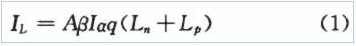
Where A is the pn junction area, q is the electron charge, Ln and Lp are the diffusion lengths of electrons and holes, J is the average light intensity calculated as the number of photons, α is the absorption coefficient of the pn junction material, and β is the quantum The yield, that is, the number of electron-hole pairs generated per absorption of one photon.
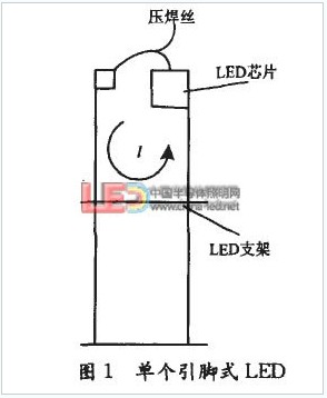
In the LED lead package process, each LED chip is fixed on the lead frame, and the LED chip forms a closed loop with the lead frame by pressure welding gold wire (aluminum wire), as shown in FIG. If the lead frame resistance is ignored, the LED holder loop photocurrent is equal to the chip photo-generated current IL. It can be seen that when the pn junction material and the doping concentration are constant, the photocurrent of the support loop is proportional to the illumination intensity I.
1.2 package defect mechanism
When the LED chip is affected by corrosion factors or contaminated with oil, a non-metal film is formed on the surface of the chip electrode to cause package defects [11]. After the electrode chip bonding process of the non-metal film layer on the surface of the electrode, a metal-medium-metal structure, also referred to as a tunnel junction, is formed at the solder joint. When a certain intensity of light is irradiated on the LED chip, if the LED chip fails, no light current flows through the support loop. If the non-metal film layer is thick enough, only a very small number of electrons can tunnel through the barrier barrier, and the LED support loop also has no photocurrent flow. If the non-metal film layer is thin, since the photo-generated current of the LED chip forms an electric field on both sides of the tunnel junction, electrons mainly tunnel through the film layer in a field emission manner, and the current flowing through the unit-area film layer can be expressed as [12].