Anti-Reverse Protection Circuit
1. Under normal conditions, the DC power input anti-reverse protection circuit uses the unidirectional conductivity of a diode to prevent reverse polarity damage. As shown in Figure 1 below: This method is simple and reliable, but it has a significant drawback when large currents are involved. For example, if a 2A current is used with a fast recovery diode like Onsemi’s MUR3020PT, which has a forward voltage drop of 0.7V, the power dissipation will be at least Pd = 2A × 0.7V = 1.4W. This results in low efficiency and considerable heat generation, requiring a heatsink for proper operation.
2. Another approach is to use a diode bridge rectifier at the input, ensuring the correct polarity regardless of how the power is connected (as shown in Figure 2). However, this solution also suffers from high power loss due to the voltage drop across the diodes. When the input current is 2A, the power consumption in Figure 1 is 1.4W, while in Figure 2, it doubles to 2.8W, making it even less efficient.
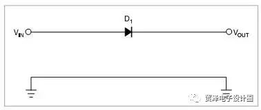
Figure 1. A series diode protection system that remains unaffected by reverse polarity. The diode has a voltage drop of 0.7V.
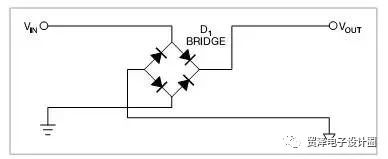
Figure 2. A bridge rectifier that works correctly regardless of polarity, but with two diodes conducting, the power loss is twice that of Figure 1.
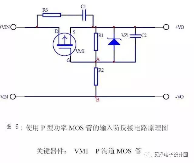
MOSFET-Based Anti-Reverse Protection Circuit
Figure 3. NMOS-based anti-reverse protection circuit.
Figure 3 shows an anti-reverse protection circuit using the switching characteristics of a MOSFET. Instead of relying on a diode, this design uses a MOSFET to control the flow of current. Since the on-resistance (Rds(on)) of modern power MOSFETs can be as low as a few milliohms, the voltage drop and power loss are significantly reduced compared to traditional diode-based solutions. In this configuration, the protection FET—either a PMOS or an NMOS—is connected in series with the load. For a PMOS, the gate is connected to ground, and the source is connected to the positive terminal of the protected circuit, while the drain is connected to the load. In the case of an NMOS, the gate is connected to the positive supply, the source to ground, and the drain to the load. When the power supply is connected correctly, the MOSFET turns on, allowing current to flow. If the polarity is reversed, the MOSFET remains off, creating an open circuit and preventing damage to the components. This method is not only more efficient but also eliminates the need for a heatsink. For example, with an NMOS transistor having an Rds(on) of 20mΩ and a current of 2A, the power loss would be (2A)^2 × 0.02Ω = 0.08W, which is negligible and does not require additional cooling. This makes the MOSFET-based solution ideal for applications where efficiency and reliability are critical.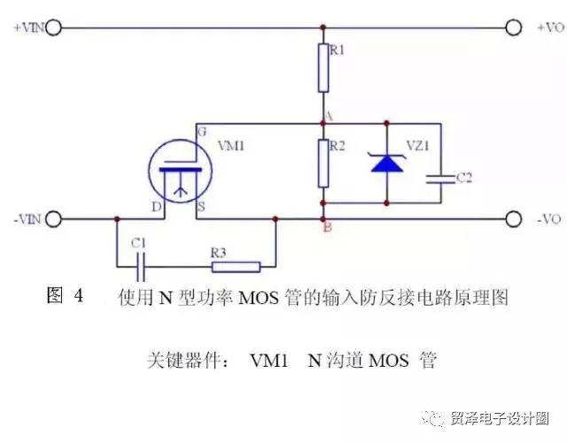
Aspheric Lens,Standard Aspheric Lens,Positive Meniscus Lenses,High Precision Aspheric Lens
Danyang Horse Optical Co., Ltd , https://www.dyhorseoptical.com