The AD604 is a low noise, high precision, dual channel, variable gain amplifier manufactured by AD Corporation. It has the advantage that the decibel number of the gain is proportional to the gain control voltage, and is especially suitable for the application of the time gain compensation circuit in the ultrasonic instrument. This paper introduces the characteristics, structure and usage of the AD604, and introduces a typical application circuit based on the ultrasonic attenuation compensation of the chip.
The AD604 is a product of Analog Devices (AD Corporation). Compared with similar products, the AD604 has ultra-low noise, high precision, continuously adjustable gain, and the decibel (dB) of gain is proportional to the gain control voltage. The time gain control (TGC) circuit of medical ultrasonic instruments requires that the gain be exponentially related to the control voltage, that is, the decibel (dB) of the gain is linear with the control voltage. Therefore, in this respect, the AD604 is an ideal ultrasonic TGC amplifier that effectively reduces the dynamic range of the signal sent to the A/D converter. The main features of the AD604 are as follows:
â—With ultra-low input noise, the voltage and current noise are respectively at maximum gain
â— Bandwidth is 40MHz (-3dB);
• has two independent gain channels, and the number of decibels (dB) of the gain is proportional to the gain control voltage;
â— The gain of each channel can be programmed. When the preamplifier is 14 dB, the gain can be adjusted from 0 to +48 dB; and when the preamplifier is 20 dB, the gain is adjustable from +6 to +54 dB;
◠has a 300kΩ input resistance;
â— Variable gain range is 20 ~ 40dB / V;
â— When the temperature and supply voltage change, the gain is very stable;
â— Single-ended unipolar gain control is available;
â— When the gain exceeds the lowest limit, the power will be automatically powered off;
â— Directly drive the A/D converter.
1 pin function
The AD604 is available in a 24-pin package and is available in DIP, SSOP and SOIC packages. The pinouts are shown in Figure 1. The function description of each pin is as follows:
PAI1/PAI2: preamplifier positive input;
PAO1/PAO2: preamplifier output;
FBK1/FBK2: preamplifier feedback terminal;
COM1/COM2: signal ground; when it is connected to the positive power supply, the preamplifier channel is turned off;
-DSX1/-DSX2: differential attenuator signal input negative terminal;
+DSX1/+DSX2: differential attenuator signal input positive terminal;
VGN1/VGN2: Gain control input and power off terminal. When grounded, the attenuation channel is turned off; otherwise, as the positive voltage increases, the gain will gradually increase;
VREF: Gain control file for both channels. When the voltage is +2.5V, the gain is 20dB/V, and when the voltage is +1.67V, the gain is 30dB/V;
VOCM: The common mode signal control terminal of the output signal. Used to determine the median voltage of the DC signal in this part of the circuit;
OUT1/OUT2: signal output terminal;
VPOS/VNEG: Connect positive/negative power supply;
GND1/GND2: Ground.

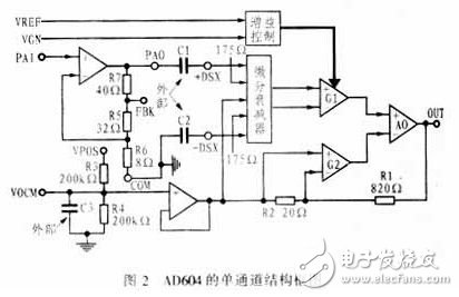
2 internal structure and working principle
The AD604 is a dual channel variable gain amplifier. Each of its channels consists of a low noise preamplifier and a variable gain amplifier (XAMP). At the same time, XAMP consists of a high precision controlled differential attenuator, a gain control unit, a fixed gain feedback amplifier and a VOCM common mode voltage control unit consisting of discrete components R3, R4. The principle is shown in Figure 2. Each channel of the AD604 provides a variable gain range of 48dB.
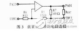
2.1 preamplifier
Each channel of the AD604 has a high performance preamplifier that can be controlled from +14dB to +20dB through an external resistor on the feedback loop. The internal circuit of the preamplifier is shown in Figure 3. Among them R5, R6, R7 are the gain control resistors of the preamplifier. The specific gain can be determined by the resistance between FBK1 and PAO1.
Small computer system interface (SCSI) is an independent processor standard for system level interfaces between computers and intelligent devices (hard disks, floppy drives, optical drives, printers, scanners, etc.). SCSI is an intelligent universal interface standard.
SCSI-3
In 1995, the more high-speed SCSI-3, called ultrasci, was born, and the data transmission rate reached 20MB / s. It increases the synchronous transmission clock frequency to 20MB / s and improves the data transmission rate. If 16 bit wide mode is used, the data transmission rate can be increased to 40MB / s. This version of SCSI uses a 68 pin interface, which is mainly used on hard disks. The typical characteristic of SCSI-3 is that the bus frequency is greatly increased and the signal interference is reduced to enhance its stability.
There are many models of SCSI-3. Ultra (FAST-20) has a transmission frequency of 20MHz, a data bandwidth of 8 bits and a transmission rate of 20MBps
Ultra wide has a transmission frequency of 20MHz, a data bandwidth of 16 bits and a transmission rate of 40mbps
The transmission frequency of ultra 2 is 80 MHz, the data bandwidth is 16 bits, and the transmission rate is 80 Mbps
The transmission frequency of ultra 160 is 80 MHz, the data bandwidth is 16 bits, and the transmission rate is 160 Mbps
The transmission frequency of ultra 320 is 80MHz, the data bandwidth is 16 bits, and the transmission rate is 320mbps
The transmission frequency of ultra 640 is 160MHz, the data bandwidth is 16 bits, and the transmission rate is 640mbps
Plastic SCSI Cover
ShenZhen Antenk Electronics Co,Ltd , https://www.antenkwire.com