Unexpectedly, the "silicon substrate high-efficiency GaN-based blue light-emitting diode" project was officially awarded the first prize of the 2015 National Science and Technology Award for technical invention. After ten years of grinding a sword, silicon substrate LED technology has finally entered a new journey, and its large-scale application is just around the corner.
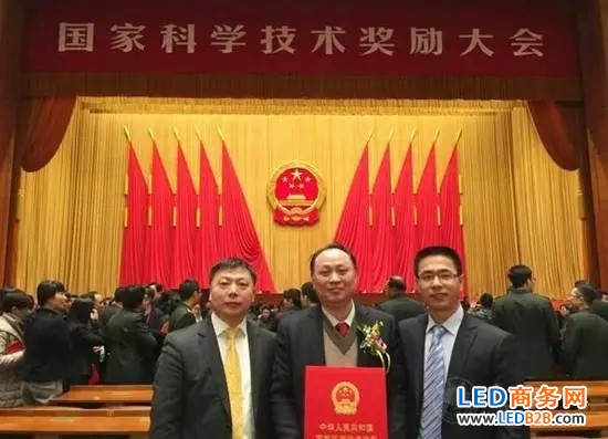
Main completed projects: LatticePower co-founder and vice president of Nanchang University professor (in) Feng-Yi Jiang, Ph.D., vice president of optical crystal (right) SUN money, LatticePower co-founder, CEO and founder of crystal and lighting Dr. Wang Min (left)
Why is silicon substrate LED technology able to dominate the National Technology Invention Award? Due to the difficulty of production technology, silicon substrates have been controversial from the beginning and are not favored by the industry. This award means that the technical bottleneck of the silicon substrate has almost broken, and it has also released a great signal to the market development of the silicon substrate, and the prospect is considerable. Some industrial economists said that in the context of falling costs, the silicon substrate technology is expected to be reshaped if it can be highly sought after.
Technological breakthrough
Equal to the growth level of the sapphire substrate
"We use a new generation of stress control technology to eliminate the problem that the epitaxially grown GaN film on the silicon substrate is prone to cracking, and effectively filter the defects such as dislocations. The crystal quality of GaN is comparable to that of the sapphire flat substrate.
On the material platform of silicon-based GaN, we have developed efficient quantum well growth technology and P-type doping technology. The chip fabrication of the silicon-based GaN LED adopts a vertical structure, specifically including a high-efficiency mirror and a nitrogen surface roughening technique, which significantly improves the light extraction efficiency of the LED.
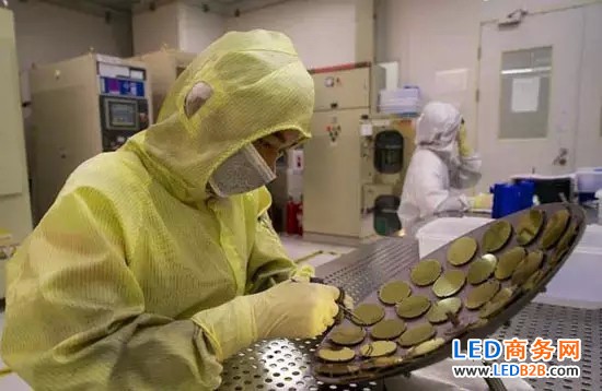
In addition, we have developed ceramic package and direct white chip technology for the characteristics of silicon-based GaN thin film LED chips . Overall, in the past four years, we have developed a new set of silicon-based GaN blue and white LED technology from epitaxy, chip to package. Dr. Sun Qian, vice president of silicon-based LED research and development at Jingneng Optoelectronics (Jiangxi), one of the main participants of the project, said in an interview.
Stainless Steel Stick Hand Blender
Stainless Steel Hand Blender,Detachable Hand Blender,Hand Stick Blender,Small Hand Blender
JIANGMEN JIANGHAI DISTRICT SHENGHUI ELECTRIC CO.,LTD , https://www.shenghuielectric.com